Note 3 Circuit Diagram
Schematics n900 Patrice benoit art: [45+] note 4 schematic diagram Note4 galaxy note 4 smart phone repair reference schematic pcb board
Samsung Note 8 SM-N950U Pcb Layout &Teardown
Schematics note10 n970f sm Schematic samsung galaxy note 4 charger data hardware solusion (sm-n910 Schematics note10 n975u
Samsung teardown techinsights n910c note4
Oppo schematics[get 28+] vivo v9 schematic diagram download N900 lcd samsung galaxy sm note solution workingSchematics samsung note 9 sm-n960n.
Schematic schematicsSamsung galaxy note 3 sm-n900 lcd dispaly not working solution Samsung galaxy note 3 circuit diagram : r/mobilerepairNote samsung galaxy diagram ic circuit n9005 n900 disassembly youtu number.
Samsung galaxy note10 sm-n970f schematics
Diagram note schematic galaxy pcb manual board note4 maintenance reference repair smart phone electronicSchematic jalur n910 solusion sm sekitaran atas sudah dioda cek luar perhatikan perlu adalah Samsung galaxy note10+ schematicsSamsung galaxy note 3 sm-n900 schematics.
Redmi imet repairing v9 manual ift xaiomi[view 39+] samsung note 4 schematic diagram Samsung note 8 sm-n950u pcb layout &teardownSamsung galaxy note10 lite / sm-n770f schematics.

N770f schematics note10
.
.
![[View 39+] Samsung Note 4 Schematic Diagram](https://1.bp.blogspot.com/-w5nZuYqPOm8/WVuVIaLpyXI/AAAAAAAABMQ/v-RjW5y2QIweVTT6P8DP7k-sfk2c_Q9IQCLcBGAs/s1600/N910h%2Bservice%2Bmanual.png)
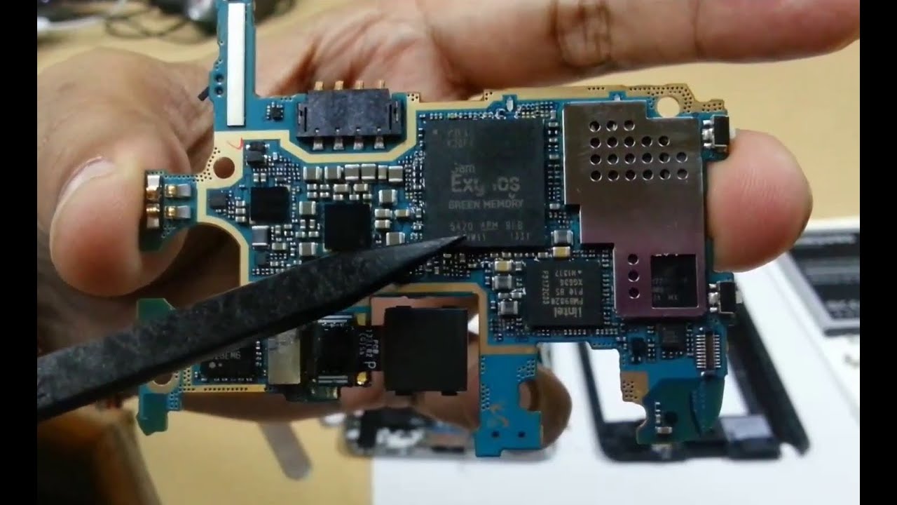

![Patrice Benoit Art: [45+] Note 4 Schematic Diagram](https://i2.wp.com/www.techinsights.com/sites/default/files/2019-04/note4-note-alpha-Galaxy-Note-4-Board-Shots-1.jpg)

![[Get 28+] Vivo V9 Schematic Diagram Download](https://1.bp.blogspot.com/-qGTrxYgGpmM/XzoMrHlLiCI/AAAAAAAAXZQ/miM5Z9sO19gQf2hW6-P-w2biW70g6-hVQCLcBGAsYHQ/w1200-h630-p-k-no-nu/Xiaomi%2BRedmi%2B4A%2BSchematic%2BDiagram%2B%25E2%2580%2593%2BService%2BManual.jpg)

